Property Of Cmos Logic Gates
Properties of dual static complex CMOS gates I Rail-to-rail excursion. CMOS Logic Gates.
 Basic Logic Gates
Previously we discussed the simplest forms of CMOS gates inverter and.
Property of cmos logic gates. 200 DESIGNING COMBINATIONAL LOGIC GATES IN CMOS Chapter 6 A transistor can be thought of as a switch controlled by its gate signal. Typically 3 to 15 volts versus 475 to 525 volts for TTL. CMOS or complementary metal oxide semiconductor logic gates are based upon metal oxide semiconductor field effect transistors.
Or conversely you get a lot of logic for the size cost and power. CMOS Logic EE141- Spring 2003 Lecture 14 EE141 Static Complementary CMOS VDD. Advantages of CMOS Logic Gates.
Lowest power dissipation of all gates a few nW. CMOS gates are very simple. A PMOS transistor acts as an inverse switch that is on when the controlling signal is low and off when the controlling signal is high.
CMOS Properties Full rail-to-rail swing. 6884 Spring 2005 2072005 L03 CMOS Technology 1. On the other hand for logic 0 input T 1 will be off and T 2 will be on thus connecting the output node to the higher voltage V DD.
CMOS gates are able to operate on a much wider range of power supply voltages than TTL. 6884 Spring 2005 2072005 L03 CMOS Technology 16 Generic Static CMOS Gate For every set of input logic values either pullup or pulldown network makes connection to VDD or GND If both connected power rails would be shorted together If neither connected output would float tristate logic VDD IN1 V IN OUT 2 INn Pullup network. 552 CMOS NAND Gate.
This post answers the question What is CMOS gate logic. Currently computer chips operating at or more than 4 GHz are available in the open. For this network if all the inputs are high the NMOS transistors will be on the PMOS.
Notice that there is no protective resistance. Layout-of-logic-gates Digital-CMOS-Design CMOS-Processing-Technology planar-process-technologySilicon-Crystal-Growth Twin-tub-Process Wafer-Formation-Analog electronic circuits is exciting subject area of electronics. YABC Therefore the inputs to this logic gate should be A B and C ie A B and the complement of C.
In this video we will learn about CMOS logic gates or CMOS logic familyWe will design CMOS logic Circuits We will design CMOS logic gates such as NAND gate. A 1 or Vdd or HIGH state b 0 or ground or LOW state c Crowbarred or ContentionX d None of the mentioned View Answer. Large noise margin I Logic levels do not dependon the size of the devices ratioless logic I Steady-state path from output to VddGnd.
Extremely large fan-out capability 50. It is a mature robust technology. High noise margins Logic levels not dependent upon the relative.
Dopantsadded to modify materialelectrical properties P P B B - -group V element ion group III electron hole n-type Donor p-type Acceptor ion free carrier free carrier n-type n add elements with extra an electron N d conc. No static power dissipation I Delay depends mainly on the load capacitance. Lower propagation delay than NMOS.
11142004 Example Another CMOS Logic Gate Synthesisdoc 24 Jim Stiles The Univ. This together with the low power consumption means it lends itself well to dense integration. Of EECS And thus.
A CMOS two-input NAND gate is shown in Figure 58. The ouput is low if eitherA AND B are both high OR C. Higher speed than NMOS.
Note that this Boolean expression says that. L CMOS Technology and Logic Gates poly Only 15432758 more meta pdiff ndiff mosfets to do. A CMOS gate is a system consisting of a pMOS pull-up network connected to the output 1 or V DD and nMOS pull-down network connected to the output 0 or GND.
Very high noise-immunity and noise-margin typically V DD 2 4. When both nMOS and pMOS transistors of CMOS logic gates are ON the output is. Transistor to transistor logic or TTL logic gates are a family of gates which bases itself upon bipolar transistors.
Intrinsic delay of all static CMOS gates Logical effort of a gate presents the ratio of its. Static CMOS Circuit At every point in time except during the switching transients each gate output is connected to either V DD or V SS via a low-resistive path The outputs of the gates assume at all times the. An NMOS switch is on when the controlling signal is high and is off when the controlling signal is low.
It is a mature robust technology. The basic gate is an inverter which is only two transistors. Schematically a CMOS gate is depicted below.
CMOS gates tend to have a much lower maximum operating frequency than TTL gates due to input capacitances caused by the MOSFET gates. Low output resistance I Very high input resistance input DC current ˇ0 I No direct path between Vdd and Gnd.
 Universal Logic Gates And Complete Sets
 Some Common Applications Of Logic Gates Electrical4u
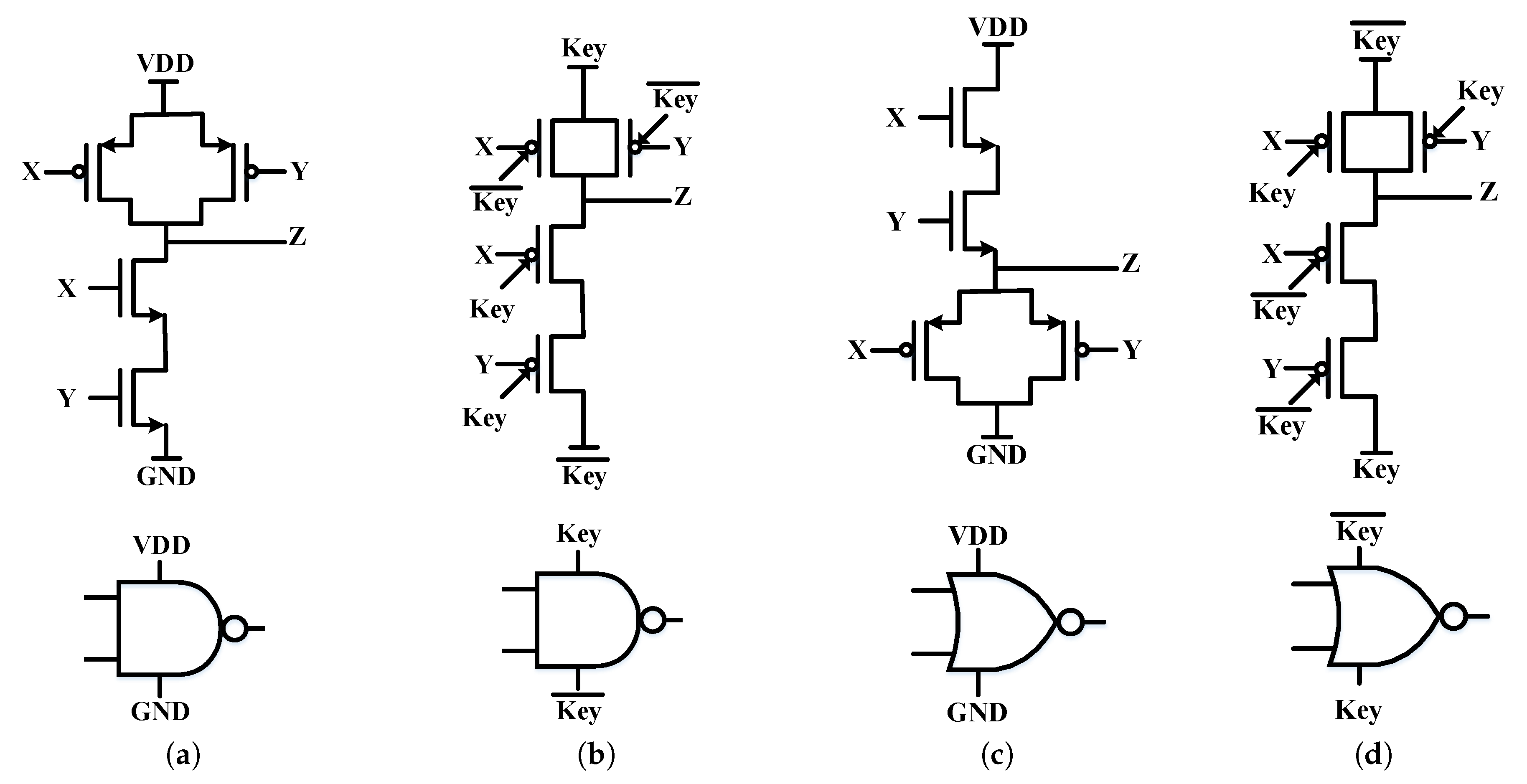 Electronics Free Full Text Logic Locking Using Hybrid Cmos And Emerging Sinw Fets Html
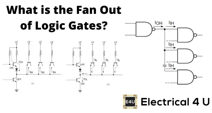
Fan Out Of Logic Gates Electrical4u
 Introduction Of Logic Gates Geeksforgeeks
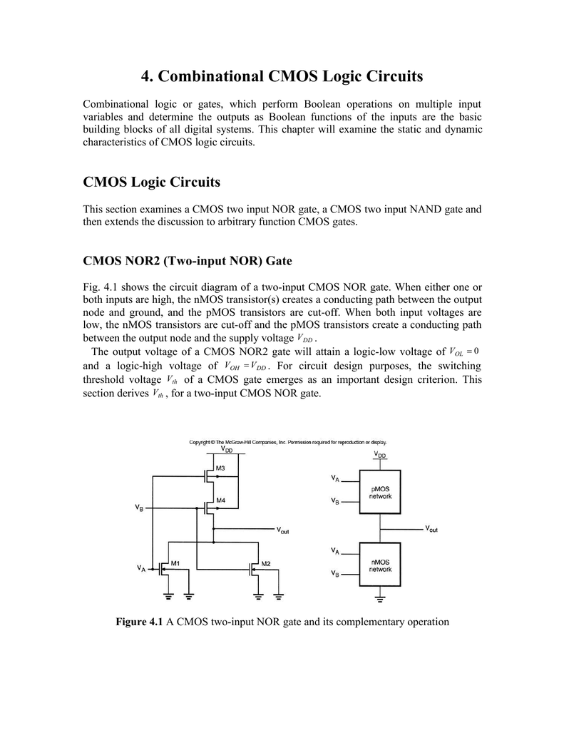 4 Combinational Cmos Logic Circuits
 Boolean Algebraic Properties Boolean Algebra Electronics Textbook Electric Circuit Ladder Logic Electronics Basics
 Diode Logic Gates Or Nor And Nand Youtube
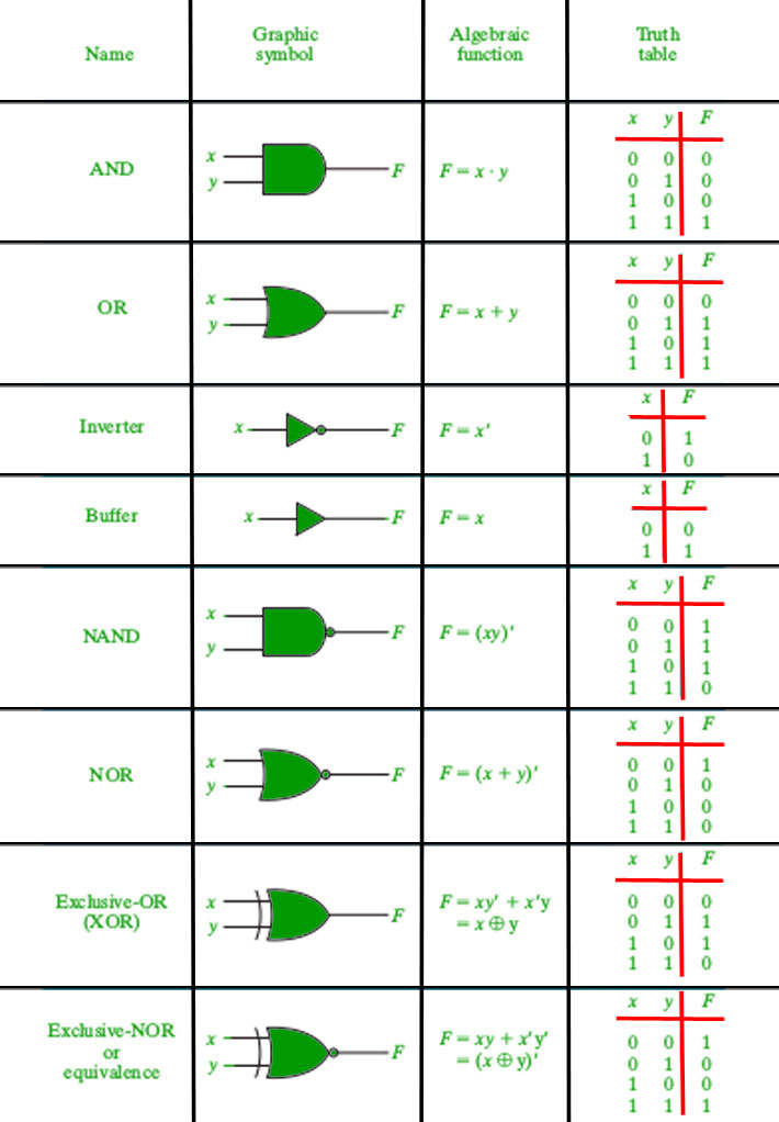
 Electrical Engineering World Logic Gates In Details Name Graphic Symbol Algebraic Function Truth T Discrete Mathematics Logic Physical Science High School
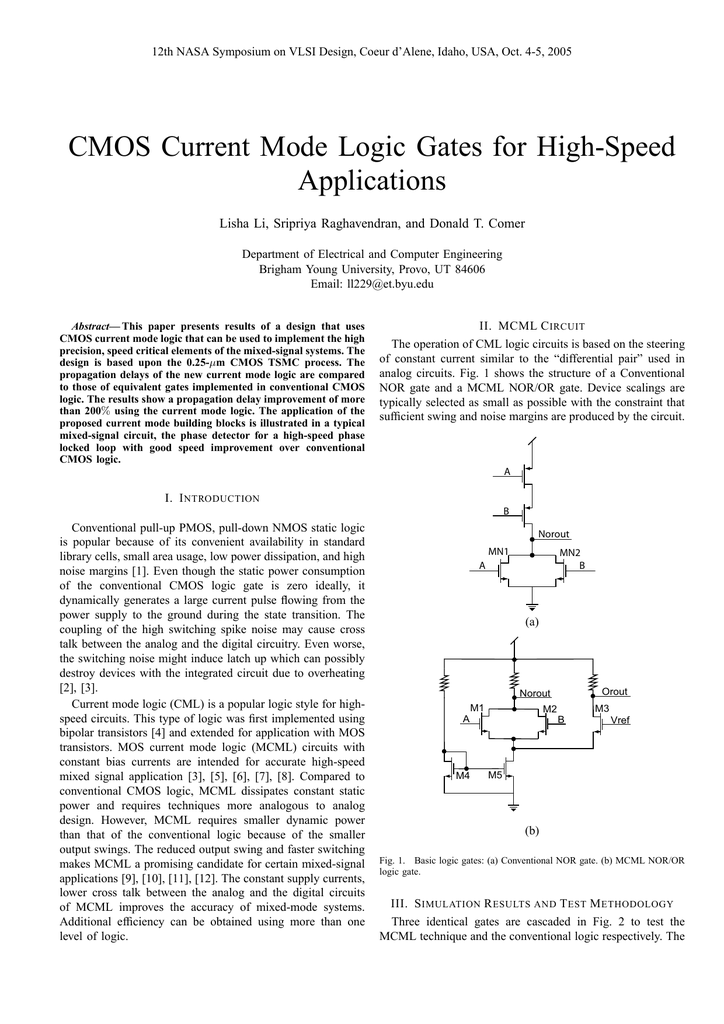 Cmos Current Mode Logic Gates For High Speed
 5 5 Cmos Logic Gates Introduction To Digital Systems Modeling Synthesis And Simulation Using Vhdl Book
 Digital Logic And Embedded Systems Smart People Use Logic To Craft Machines Blog Octopart
 7404 Logic Not Gate Logic Electronic Engineering Electricity
 The New Marriage Logic By Don Mcmillan Logic Electrical Symbols Symbols
 Logicly A Logic Circuit Simulator For Windows And Mac Logic Gates Flip Flops Computer Architecture Logic Design Circuit Simulator Computer Architecture
 Logic Gates Make Up All Things Digital This Tutorial Will Cover The Basic Logic Gates And How They Work Along With Truth Tables Learn Physics Tutorial Logic
 Pin On Circuits
 Cmos Logic Gates Worksheet Digital Circuits